
Solar Panels
Anatomy of solar cells
Photovoltaic, or solar cells - is a combination of semiconductors with different type of conductivity. Fine, but what does it mean "semiconductors", and what does it mean "conductivity"?
Let's first talk a little about the Elementary Theory of Semiconductors.
Semiconductors - is a group of tetravalent elements (Valence - is the number of electrons, which an atom can acquire or lose), located in the middle of the periodic table. They are neither good conductors, nor good insulators.
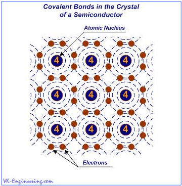
Figure 1
As shown in Figure 1, the crystal lattice of the semiconductor elements is formed by tetravalent atoms linked together by covalent bonds (Covalence - a measure of the ability of atoms to form chemical bonds that arise due to two electrons (one from each atom). In chemical compounds with the covalent bonds, the valence of atoms is determined by the number of generated "shared" electron pairs).
Initially, in the semiconductor technology, a prominent place was occupied by elements such as germanium (Ge) and silicon (Si). Currently, the greatest preference is for silicon. For example, more than 95% of all solar cells, currently produced worldwide, are based on this, one of the most common in the earth's crust, the chemical element. The most promising materials for solar cells, is silicon - Cu(In,Ga)Se2, and gallium arsenide (GaAs), with the structure of AlGaAs-GaAs.
In order to get semiconductors suitable for the production of solid-state semiconductor devices, it is necessary to add some impurities (doping). There are two types of semiconductors, mainly differing by the type of conductivity caused by impurities. In the semiconductors of n-type, current is carried by negatively charged carriers, while in p-type semiconductors - by positively charged ones.
The n-type semiconductors are produced by adding impurities, that can "give away" free electrons into the crystal lattice of pure semiconductor. So, in order to get a free electron, necessary for getting the semiconductor of n-type, it is needed to add a small amount of pentavalent impurity (Fig. 2), for example, antimony (Sb). In this case, not much doping is required - just about one part impurity for 100,000,000 parts of the semiconductor.
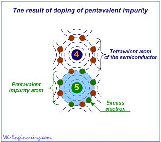
Figure 2
Atoms of the pentavalent impurity, in turn, form covalent bonds with tetravalent atoms of the crystal lattice of the semiconductor. Thus, on each impurity atom, one electron is released, and if some voltage is applied to the crystal, then there is an electrical current. Let's memorize: In the semiconductor n-type, electrical current is created by the movement of electrons.
Semiconductors of p-type
P-type conductivity in the semiconductors, is called the "hole conduction". Hole - is a place in the crystal lattice where an electron should be located, but actually it is not there - briefly and clearly. Graphical explanation of this phenomenon is presented in Figure 3.
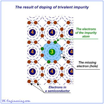
Figure 3
When a trivalent atom of the impurity, for example, Gallium (Ga), takes its place in the crystal lattice of the semiconductor, beside him, there is an atom that cannot create a covalent bond because the other atoms have already formed bonds with all three electrons of the impurity. So, the place, where the "missing" electron should be located (if the valence of the impurity is equal to four), - is determined as the hole.
However, how the holes could carry an electric current? It is, after all, just an empty space! Actually, the holes, by themselves, do not carry electrical current, - this is just an impression. From time to time, this free space (hole) is occupied by the electron, but at the same time elsewhere in the crystal lattice, in turn, formed a hole. Let's look at Figure 4.
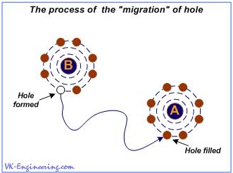
Figure 4
Let's suppose that in the beginning, there was a hole in the atom "A". Under the influence of an electric field (e.g. voltage), an electron from the atom "B" is released. The field causes the electron to move to the point where it can be captured by the atom "A". Thus, the hole in the atom "A" is filled, but it is formed in the atom "B". It creates an impression of moving hole, but in fact, this is an electron moving. The holes can be seen as positively charged particles of the same size as the electrons. Although it is only commonly accepted interpretation - in most cases it is convenient to use, so I advise you to accept it.
p-n junctio
When two semiconductors, n- and p-type, are joined together, there is a diffusion of charge carriers with different type of conductivity in the area of their contact. After the diffusion, in the p-zone, near the contact area, there are accumulations of non-mobile negative charges, and in the n-zone - the positive ones. Thus, a region of space charge, consisting of two oppositely charged layers is formed. As a result, an electric field, which precludes further diffusion of majority charge carriers through the contact's area and establishes the equilibrium condition, is created. (Fig. 5).
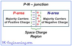
Figure 5
Let's take a look how it all works in the simplified example, illustrating the work of the diode.
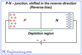
Figure 6
If a battery is connected as shown in Figure 6, i.e. the positive terminal of the battery (+) is connected to the n-region, and the negative one (–) is connected to the p-region of the semiconductor, then, in our device, the following occurs: The negative charges (electrons) of the n–type semiconductor will flock to the positive terminal of the battery, and positive charges (holes) of the semiconductor of p–type – will flock to the negative one. Then, in the area of the p–n-junction, a wide zone with no carriers is formed. This zone is called depleted zone. The current through the p–n-junction is created by electrons and holes, which interact, neutralizing each other. Thus, if Depletion Zone becomes sufficiently wide, current flow is terminated. In this case, we say that p–n-junction is shifted into reverse. Figure 7 shows the p–n-junction shifted in the forward direction due to change of the polarity of the battery. As you can see, in this case, the negative terminal of the battery is connected to the n–semiconductor, and positive one - to the semiconductor of p–type.
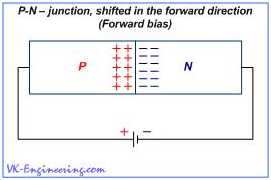
Figure 7
So, output electrodes of the battery push away the charges, which begin to accumulate in the zone of p–n-junction. As a result, the current through the junction increases significantly, as more electrons and holes begin to interact. Battery "injects" more and more electrons into the n-region, and its second - positive output creates more and more holes. Of course, you can ask: "Why to dwell on the theory of semiconductors, and how the diode works?" The answer is simple. Work of the photovoltaic cells, used in the solar modules, is based on the same principle, as in a diode. With only one essential difference, - in order to excite an electric current in the solar cells, not energy of the electric field created by the voltage is used, but rather the photons energy, which causes the so-called photovoltaic effect.
As mentioned on different article, "The photovoltaic effect in a semiconductor material occurs when the photon can convey to a valence electron (electrons located on the outer, or valence shell of the atom) the amount of energy, enough to move it into the conduction band.". Due to this phenomenon, the light, to a certain extent, affects the conductivity of the p–n-junction and origination of the electric charge. This effect is observable even in the ordinary glass diodes.
Photovoltaic cell, in the simplified form, is a two-layer system (sandwich), composed of semiconductors of different conductivity type, with the p–n-junction of a large area. (Fig.8).
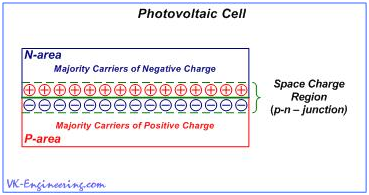
Figure 8
When the light, in the form of photons, hits our solar cell, photon energy frees the couples "electron-hole". Each photon, that has a sufficient energy, as a rule, frees only one electron and one hole, respectively. As a result, free electron and hole begin to wander within their areas, and the electric field directs them to appropriate zones - electrons in the n-region, and holes in the p-region. This leads to disruption of the equilibrium state, and if we provide an external path (circuit) for the flow of electrons toward the p-region, then, by the way, they will do work for us. (Figure 9). The flow of electrons provides the current and electric field - voltage.
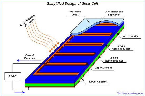
Figure 9
Electric charge, which appears in the photovoltaic cell as a consequence of impact of solar radiation, is directed to output contacts in the form of low DC voltage. Semiconductor materials have a reflectivity, and as a result, some numbers of the photons reflects from their surface, and are not involved in the conversion process. In order to reduce these losses, the anti-reflection coating, or film, is used.
The output voltage of the silicon photocell is approximately 0.5 volts, so, in order to get the necessary value of voltage, solar cells assembled into the modules (panels). Module typically consists of 36 solar cells connected in series. The most common value of the output voltage at the output of the module is 12 volts (specified value) - although the effective output voltage is higher than 17 volts (rated or operating voltage). This is the same as the generator of your car charges 12-volt battery with voltage exceeds 12 volts. So, there is always a difference between the specified and operating voltage.
The solar panel output power is stated in watts, and is determined by multiplying the rated voltage of the module at its rated current, Pout = U x I. For example, the solar panel BP380 at 12 volts, 80 watts (produced by "BECO Solar" the company), with dimensions – 1,204 x 537 millimeters, has a rated voltage - 17.6 V and rated current - 4.55 A.
Hence:
17.6 x 4.55 ≈ 80 watts
We know, that the solar radiation intensity is unstable and varies during a day. Early in the morning and late in the day, the sunlight produces less energy than at the noon, and during a cloudy day will produce less energy than during sunny day. That's why, as a way of smoothing of these fluctuations, the "Peak Sun Hours" value is used. When planning the system for your geographical area, the average amount of "Peak Sun Hours" in a day is estimated according to statistical data for the whole year or at the average value for the worst month.
Thus, if the average Peak Sun Hours value for your region is equal to 5.5 hours per day, then the solar panel above mentioned can produce about of 440 watt-hours of electricity a day:
80W x 5.5 hours = 440 watt-hours
Not much, isn't it?
In order to increase the output power of the system, solar panels can be connected in series or in parallel, and also in combination - a series-parallel connection.
Solar modules - connection diagram
The series connection allows to increase the output voltage of our system. In this case, the positive terminal of one panel should be connected to a negative terminal of second one… and so on. (Fig.10).
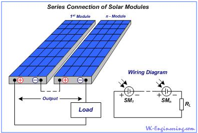
Figure 10
As a result, between the external (positive and negative) terminals (output), we will get the total voltage of two (or more) panels, but the total electric current of the panels remains the same, as the current of one. For example, with a series connection of two panels at 12 volts and 4.5 amperes, we will obtain the output voltage of 24 volts, at a current 4.5 ampere. With a series connection of four panels, we obtain at the output of 48 volts at a current of 4.5 amps. In parallel connection, the positive and negative terminals of panels are connected together, according to their polarity. (Fig.11).
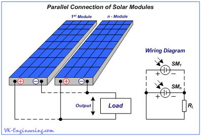
Figure 11
In this case, current strength of the panels is summarized, but the voltage value remains unchanged. Thus, two solar panels at 12 volt and current 4.5 ampere each, connected in parallel, will give at the output 12 volt, with a current 9 amps, and four panels - 12 volt with a current of 18 ampere.
Series-parallel connection is used to increase both the output voltage and output current. (Fig.12).
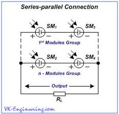
Figure 12
In addition, one group of modules can be connected in parallel to another one (and so forth).
So, use of above mentioned connection types allows us to build the systems of large capacity.